DESY Spin-off · Patented Technology

See Inside Your
Semiconductor

Our mission is to help you understand how, where and why your device excels or fails — with non-destructive 2D/3D X-ray performance mapping.

  • Works through encapsulation — no sample destruction
  • Operando: measure devices under real operating conditions
  • 2D and 3D imaging — 15 μm in the lab, down to 30 nm at the synchrotron
  • Structure and performance correlated in a single workflow

Bringing Semiconductor Analytics from the Synchrotron to the Lab

HaScI lab-scale XBIC measurement instrument with active X-ray measurement

Lab

15 μm

Lab-source XBIC

Synchrotron

30 nm

e.g. P06 at PETRA III

The Challenge

The Cost of Working Blind

A 20 EUR SiC diode can trigger a 20 million EUR recall. A 2% better PV cell yields millions in margins — and billions in market share. Without visibility into local electrical performance, semiconductor development is a guessing game.

Without our service

Blind troubleshooting

  • Performance decrease — root cause unclear
  • Late failure detection, high scrap rates
  • Trial-and-error debugging cycles
  • Slow yield ramp-up
  • No performance ground truth for design simulations

With our service

Actionable performance data

  • Structural defect ↔ electrical impact directly mapped
  • Early detection of performance losses
  • Precise root-cause localization
  • Faster yield optimization
  • Performance-informed simulations from measured data
What We Measure

Unique Capabilities

Our XBIC platform covers what no other lab-scale technique can — from sealed packages to operating conditions to full 3D performance maps.

Through Encapsulation

Through Encapsulation

X-rays penetrate the package. Measure electrical performance of sealed, encapsulated devices — without opening or destroying them.

During Operation

During Operation

Operando measurements with the device powered and active. Observe how real operating conditions affect local charge collection and performance.

3D Tomography

3D Tomography

Full volumetric 3D XBIC imaging. Locate defects and performance variations not just on surfaces but at depth — across the full device volume.

Structure + Performance

Structure + Performance

Correlate structural data (density, composition, lattice) directly with local electrical performance maps. Understand how and why a device works.

The Method

Mapping Performance in 3D

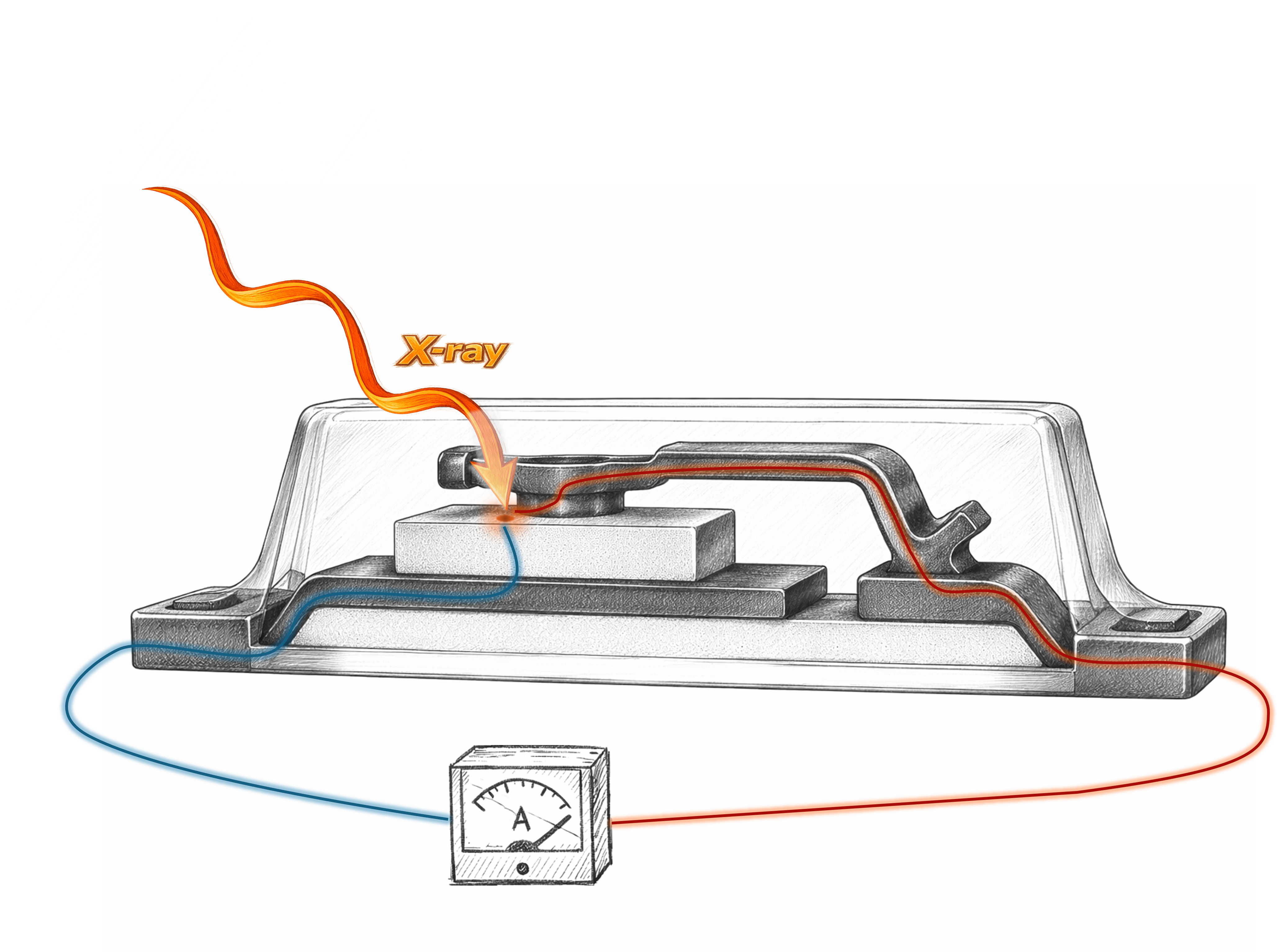
Our most unique technology is X-ray Beam Induced Current (XBIC). We use a focused X-ray beam to locally generate electron-hole pairs inside a semiconductor device. Ordinarily, these quickly re-combine. Only in the active charge-collection or depletion region of a diode, transistor or solar cell, an internal electric field is present that separates these pairs and allows conduction to the electric device contacts. The resulting induced current is measured synchronously as the beam scans across the sample.

The current map directly reflects the local charge collection efficiency from the perspective of the real device contacts. Any imperfections between junction and contact — be it due to material faults, contact quality, or packaging effects — show up in the measurement. This reveals where the device works well, where it is degraded, and precisely where defects reduce performance.

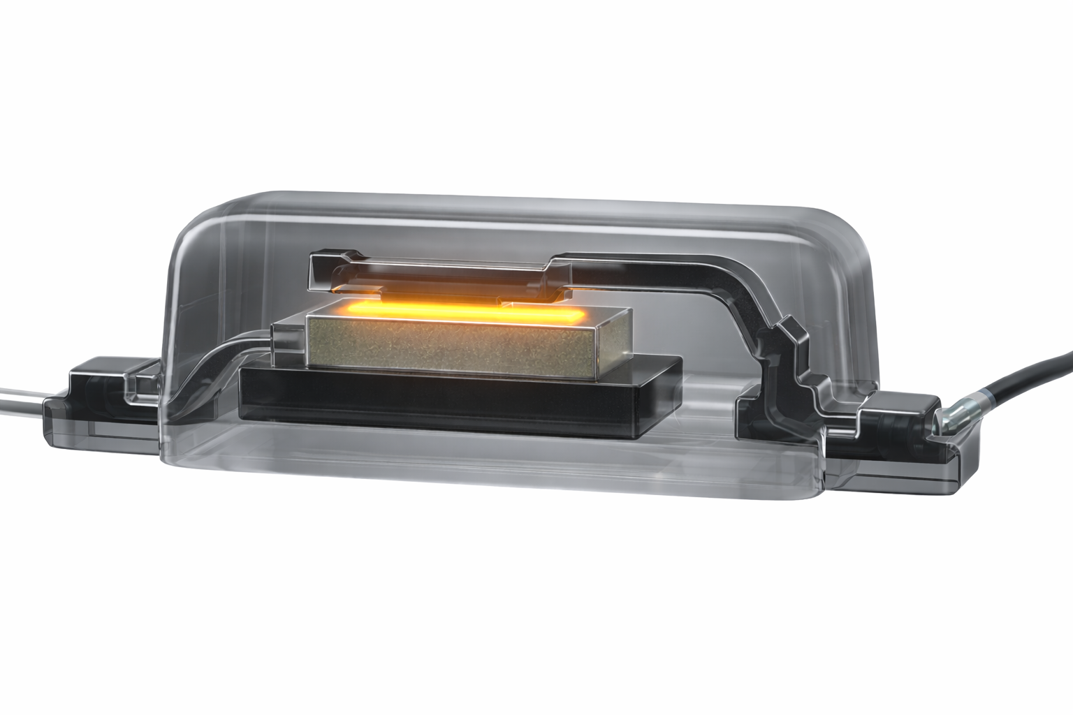
Because X-rays are highly penetrating, the measurement is fully non-destructive and works through packaging, encapsulants, and even under real operating conditions.

How it works

01 Focused X-ray beam scans the device
02 Beam generates local electron-hole pairs
03 Induced current measured synchronously
04 Performance map reconstructed in 2D or 3D
EP 4 006 530 A1 US 11,461,939
Sketch of the XBIC measurement principle: an X-ray beam hits an encapsulated semiconductor device, generating a locally induced current measured by an ammeter

A Comprehensive Picture

XBIC performance mapping combined with structural X-ray imaging forms our core offering, available today at lab scale. At synchrotron beamlines, we can already complement this with additional modalities — fluorescence, diffraction, and luminescence — to build a complete multi-modal picture of your device. We are actively working to bring these techniques to the lab as well.

Measurement Technique Availability
Structure Density X-ray absorption
Lab Sync 2D 3D
Performance Local charge collection XBIC
Lab Sync 2D 3D
Impurities & doping Atomic composition X-ray fluorescence
Sync 2D (3D)
Strain & temperature Lattice distortions X-ray diffraction
Sync 2D
Carrier lifetime Band-gap recombinations Luminescence
Sync 2D

Structure + performance (XBIC) measurements are available today at our lab. All modalities are accessible at synchrotron beamlines. Lab-scale development for extended techniques is ongoing.

What We Offer

Our Services

We intend to offer measurement services ranging from a one-off diagnostic session to a full failure investigation — working with you to design a workflow that answers your development questions.

01

Measurement Service

Turn-key X-ray and laser measurements performed by our team. Available at our lab facility and, for specialised requirements, at synchrotron facilities. You define the sample and question — we deliver the data.

  • Lab-scale XBIC (2D & 3D)
  • Synchrotron access for advanced cases
  • Laser beam induced current (LBIC)
  • Non-destructive — samples returned intact
02

Analysis & Interpretation

Raw data is only half the story. We process, reconstruct, and interpret results in the context of your device physics and development questions — delivering actionable conclusions, not just images.

  • 2D/3D performance map reconstruction
  • Correlation with structural data
  • Expert consultation on findings
  • Results report with engineering context
03

Root-Cause Analysis

When devices fail or underperform, we help identify exactly where, why, and how. Combining performance and structural measurements, we isolate electrically active defects and separate them from structural artefacts.

  • Failure localization at sub-micron scale
  • Structural vs. electrical defect separation
  • Long-term degradation analysis
  • Design and process improvement recommendations

Ready to discuss your measurement challenge?

We work with each partner individually. Pricing and scope are defined based on your specific device and question.

Get in Touch
Current Status

Market Field Study — Active

We are now engaging with semiconductor developers across Europe to understand where X-ray performance diagnostics can best contribute to real-world workflows — be it yield optimization, failure analysis, or ground-truth data for AI-assisted design. Interested in participating? We'd love to hear from you.

Participate →
Updates

News & Milestones

milestone

HaScI Launches Market Field Study

Hamburg Scientific Instruments is now actively engaging with semiconductor manufacturers, power electronics developers, and photovoltaic producers to understand where X-ray performance diagnostics can best contribute to real-world development workflows.

milestone

Perform3D: Helmholtz Validation Funding Secured

The Perform3D validation project secures ~1.47 M€ to bring 3D semiconductor defect mapping from the synchrotron to lab-scale X-ray sources together with our partner Xnovo Technologies.

Read more →
milestone

XBIC Technology Granted Patents in Europe and the United States

The X-ray beam induced current (XBIC) measurement technology developed at DESY has been granted patents in both Europe (EP 4 006 530 A1) and the United States (US 11,461,939), securing the intellectual foundation for commercial development.

Scientific Publications

Our work is grounded in peer-reviewed science. A full publications list is being assembled — check back soon.

Publications list coming soon
The Team

Who We Are

Three scientists with over a decade of X-ray method development at DESY and synchrotrons around the world — now building a company to bring this capability to industry.

Dr. Michael Stuckelberger
Co-Founder

Dr. Michael Stuckelberger

Scientist in Charge of X-ray Microscopy for Energy Materials

Over a decade of research in X-ray based semiconductor characterization at DESY and synchrotrons worldwide. Leads the scientific vision and technology development.

Dr. Evelina Ametova
Co-Founder

Dr. Evelina Ametova

Scientist for X-ray Imaging and Tomography

Expert in X-ray tomography and computational imaging. Drives 3D reconstruction methods and data analysis for multi-modal semiconductor diagnostics.

Dr. Robin Y. Engel
Co-Founder

Dr. Robin Y. Engel

Scientist for Semiconductor Performance Mapping

Specializes in synchrotron-based X-ray techniques and instrument development. Bridges fundamental science and commercially viable measurement solutions.

Institutional Affiliations & Partners

DESY Innovation & Technology Transfer
CXNS
Centre for X-Ray and Nano Science
Start-up Labs Bahrenfeld
Xnovo Technology
Xnovo Technology
Get in Touch

Let's Discuss Your
Measurement Challenge

We are actively engaging with semiconductor developers to understand where X-ray performance diagnostics can best contribute. Whether you have a specific device failure, a yield question, or simply want to explore what's possible — reach out.

The form on the right uses Formspree to send a message to Robin Engel.

Your message goes directly to the founding team. We do not share your data with third parties.

Hello wayward traveller of the digital realm. You have come to a place that is still in the making — yet raw and unfinished. You may look around, but be wary of uncharted waters. But return in the future, for maps are being drawn!